APECS pilot line

Advanced Packaging and Heterogeneous Integration for Electronic Components and Systems

© APECS
APECS consortium

The APECS pilot line at a glance:

As part of the EU Chips Act the APECS pilot line marks a major leap forward in strengthening Europe’s semiconductor manufacturing capabilities and chiplet innovation. By providing large industry players, SMEs, and start-ups with easier access to cutting-edge technology, the APECS pilot line will build a strong foundation for resilient and robust European semiconductor supply chains.


Within APECS, the institutes collaborating within the Research Fab Microelectronics Germany (FMD) are working closely with other European partners, making a significant contribution to the European Union´s goals of increasing technological resilience, strengthening cross-border collaboration and enhancing its global competitiveness in the semiconductor technologies.

APECS is the novel pan-European pilot line to establish a groundbreaking infrastructure for heterogeneous integration and advanced packaging

Europe's investment in semiconductor research, through strategic projects such as APECS in the EU Chips Act, is crucial to reduce our dependence on international supply chains that are heavily concentrated in other regions. By boosting technological sovereignty, APECS is securing Europe's long-term economic stability and positioning the EU as an indispensable partner in the technological breakthroughs that lie ahead for the digital age. Furthermore, APECS will play a pivotal role in Europe's transition towards a carbon-neutral and circular economy through its promotion on eco-design and green manufacturing initiatives.

APECS will be a key driver of collaboration among European RTOs, industry and academia, fostering a lively innovation ecosystem. Customers will benefit from a single point of contact to the APECS pilot line. APECS covers end-to-end design and pilot production capabilities, to accelerate progress from cutting-edge research to practical, scalable manufacturing solutions.

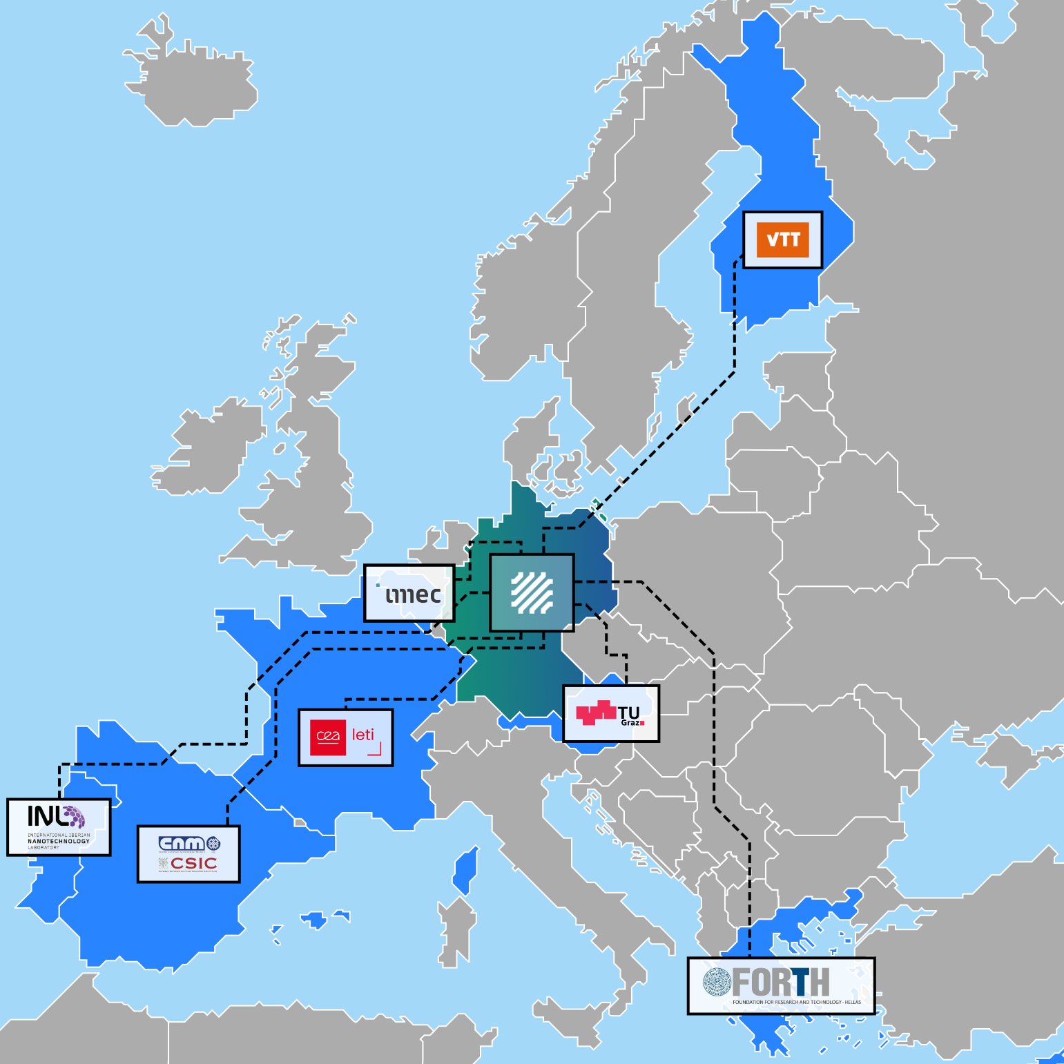
The APECS consortium brings together the technological competences, infrastructure, and know-how of ten partners from eight European countries: Germany (Fraunhofer-Gesellschaft as coordinator, FBH, IHP), France (CEA-Leti), Belgium (imec), Finland (VTT), Austria (TU Graz), Greece (FORTH), Spain (IMB-CNM, CSIC) and Portugal (INL).

Our contribution in the APECS pilot line

Chiplet integration (2.5D and 3D)

Advanced Packaging and Heterogeneous Integration for Electronic Components and Systems

An important part of APECS is 2.5 and 3D integration technologies, which are crucial for creating powerful, compact and energy-efficient systems. 2.5D integration combines the advantages of 2D and 3D technologies by placing multiple chips in a single plane connected by an interposer layer. This technique enables optimal connection and communication between the chips, improves signal quality and reduces latency. As a result, different technologies and materials can be combined efficiently, which increases the flexibility and performance of the systems. 3D integration goes one step further and stacks chips vertically, resulting in even shorter wiring connections. This arrangement allows for a significant improvement in data transfer rates and overall performance while minimizing space requirements. The reduction in signal paths also contributes to energy efficiency, which is of great importance in high-performance applications.


Research at Fraunhofer IPMS includes:

Within APECS, we are developing technologies for 2.5D and 3D integration at 300 mm wafer level in close cooperation with Fraunhofer IZM-ASSID. The aim is to enable 3D stacking of advanced CMOS wafers and non-CMOS heterogeneous/multi-material wafers. In 2.5D integration, chiplets are to be integrated directly onto interposers. These developments are particularly important for applications in the fields of neuromorphic computing, trusted electronics (e.g. security functions) and are the basis for integrated high-performance chips.

  • Ultra-High-Density (UHD) interposers
  • Passive functionalized interposers
  • 3D stack integration


Funding note

APECS is co-funded by the Chips Joint Undertaking and national funding authorities of Austria, Belgium, Finland, France, Germany, Greece, Portugal, Spain, through the Chips for Europe Initiative.

Thanks to substantial funding from the German Federal Ministry of Research, Technology and Space (BMFTR) and the federal states of Saxony, Berlin, Bavaria, Schleswig-Holstein, Baden-Württemberg, North Rhine-Westphalia, Brandenburg, and Saxony-Anhalt, it will be possible to further expand the R&D infrastructure in the coming years within the framework of the APECS pilot line.